- О программе
- Рабочее поле
- Элементы
- Функции
- Библиотека
- Дополнительные возможности
- Печать и экспорт
- Файлы для фрезеровки (экспорт HPGL)
- Создание экспортного файла для фрезерного станка (HPGL)
Создание экспортного файла для фрезерного станка (HPGL)
To describe the export functions we sketched a small sample PCB that will show all the functions of this new option.
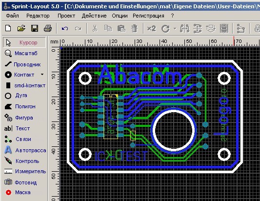
As you can see this is a double-sided PCB
Before we start the export dialog, we must decide what text on the PCB is single LINE or outline.
All text segments that are to be milled as single LINE must be highlighted before the start of the PLT option.
Since we want to store the top layer C1 (blue) first, we will highlight the text segment "IC - test", as we want it to be milled single LINE. The text segments "Abacom" and "Logo" are to be milled like our tracks outline and therefore need no further attention.
We enter the function as follows:
File - > exporting - > milling files - > isolation milling(HPGL, *plt)
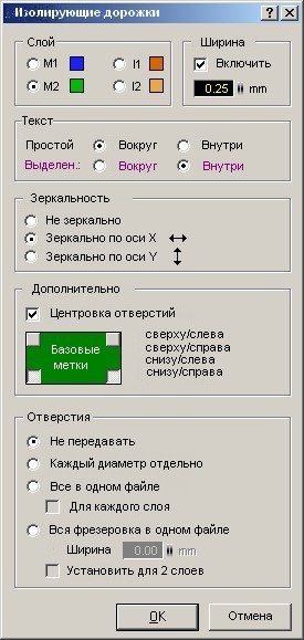
The following dialog appears:
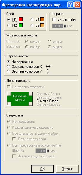
In this dialog we select the following options:
Layer
Since we want copper side 1, we select the Layer C1.
Milling Width
This is the width of the milled isolation path. It is necessary to know what the milling tool width that will be used to mill the PCB is. In our case it is 0.25mm.
Text
We select the text options for our highlighted text as "singleline", and for the un-highlighted text we select "outline"
Mirrors
Since we are dealing with the top side of the PCB layer C1, we will not need to mirror the PCB.
Options
Mark drill holes for centering
If the option "Mark drill holes for centering" is activated, all pads and eyelets receive a centering point. The milling tool will drive to the center of each pad or eyelet and mill a small hole to the same depth as the isolation path.
This function was included to allow good alignment of CNC drills during the hole drilling process and reduce the chance of the high speed hole drills from bending and breaking.
The only disadvantage of this function is an extension of the isolation milling job by the additional centering points.
In our example we decided for the centering holes.
Reference holes
The following "Reference holes" option affects all files that are used in the manufacturing of our PCB.
You can set several alignment holes for our PCB. It is important to remember that these alignment holes appear at the same place in all files.
That means: The zero point of the individual Layers are always alike.
Drillings
The last part in this dialog is dedicated to producing the hole drilling PLT files. This option is perfect for those who don't have the Excellon function on there milling software. Sprint layout can produce Excellon files if need, this function can be found under the following menus, export, Drill data (Excellon).
As our PCB has two different hole diameters (0,6 and 0.8 mm), we select the option "Each diameter in a extra file" this will produce a PLT file for each hole size.
We confirm our selections with OK.
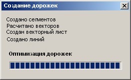
The following window indicates the progress of the outlining production.
Next we get a save file dialog.
Here we give a name and destination directory for the PLT files "Sample C1.PLT".
The drilling files are put in the same directory. The drill files are automatically named and are self-describing.
Now we will deal with the back C2 (green) layer of our PCB. Again all text segments that are to be milled as "singleline" must be highlighted before the start of the PLT option.
Like before we select the "isolation milling" option.
This time we select the Layer C2.
The milled isolation path width and text attributes should still be set from the previous time.
We will select to reflect "Mirror horizontal" to reverse the PCB output as we are milling from the bottom and not the top.
Our options for "Reference holes” have also been copied over from the first layer setup.
As we have already made our drilling files from the C1 side, we will deactivate "Mark drill holes for centering" and we will select "No output” for the Drillings options.
We confirm our options with OK and again we are presented with a file dialog.
Here we see the files that were produced previously. We want to store our C2 side in addition to these. So we give a name for the C2 PLT files "Sample C2.PLT”.
Producing a PCB outline PLT file
Last of all we want to mill our PCB outline, mounting holes and any cutouts. This can be accomplished easily in a milling job with Sprint-Layout.
You will have to draw the outline of your PCB, mounting holes and any cutouts on the outline layer O (white). You can only use tracks, circles and polygons to draw your outline. All other elements e.g. pads are ignored by the PCB Outline Milling function.
The zero point or reference holes of the milled isolation and drilling files from our project are used here also. Thus it is possible to mill the PCB outline after the C2 layer has been milled (after appropriate milling tool change) with out repositioning the PCB.
Note: the PCB perimeter outline is milled in the center of the drawn track so it is important to select a track width that is the same as the milling tool that will be used to mill the PCB.
Looking at our sample PCB again.
We have our PCB-outlined on layer O (white). Our PCB has 4 mounting holes (5,5mm), a round outbreak (16mm) and the outer contour. The exact diameter of the holes we can configure in the properties-panel after selecting the circle:
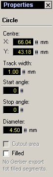
During the input of the diameter note that you must include the width of the drill. Since the tool will mill concentrically around the radius, the milled hole width will be wider. You must take the milling tool width off from the diameter of the hole, in order to obtain the correct hole width result.
In our case we want a hole of 5,5mm and our milling tool has a width of 1mm. The input in the circular arc dialogue diameter must therefore be 4.5 mm.
If you draw PCB outlines, make sure that you first draw outbreaks, and holes within the PCB outline then draw PCB outline. Remember, what was drawn first will also be milled first.
We first highlight all elements that are going to be used to produce the PCB outline, cutouts and holes.
We start the dialogue as follows:
File - > exporting - > milling files - > PCB Outline milling(HPGL, *plt)
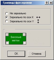
Since we want to mill the PCB outlines from the back of our example PCB C2, the outline (like C2) must be mirrored. We select "Mirror horizontal".
The "Reference holes" were copied over automatically.
We click on OK and are presented again with our file dialogue.
We name our plate outline file "Outline.PLT" and click again on "Save".
Now we have all the files required to manufacture our PCB on a milling plotter.
- Sample C1.PLT Copper side C1, PCB top
- Sample C2.PLT Copper side C2, PCB bottom
- Outline.PLT PCB outlines, cut outs and mounting holes
- DRIL_60.PLT PCB pads that have 0.6 mm holes
- DRIL_80.PLT PCB pads that have 0.8 mm holes