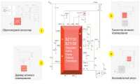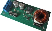

95-Ваттный преобразователь напряжения для ноутбука 12В -> 19В 5А
Если использовать портативный компьютер или ноутбук вдали от электросети, то батареи рано или поздно придется зарядить. Автомобильное гнездо прикуривателя в автомобиле - также электрический выход, но только 12 V. Но для нас это не проблема; соберем Адаптер, описанный в этой статье. Адаптер может дать достаточное напряжение и ток для сегодняшних портативных компьютеров от автомобильной батареи. Его легко собрать, имеет превосходную эффективность.
Параметры
• Выходной ток: 5А (10А мгновенное значение)
• Входное напряжение: 10 В - 15 В
• Частота переключения: 42 кГц
• КПД (типичное значение): 95 %
• Выходное напряжение: 19 V ± 0.5 (регулируемое) V
• Минимальное входное напряжение: 9.2 V
• Максимальная непрерывная выходная мощность: 95 W
• Размер платы: 59 мм x 98 мм
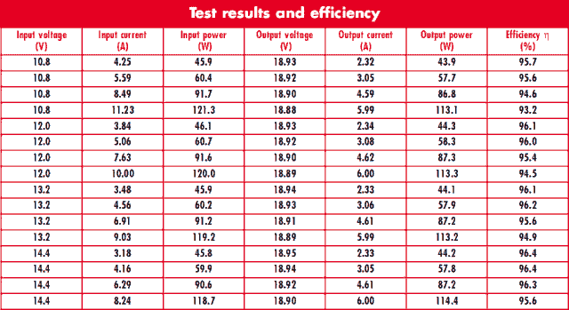
Преобразователь для ноутбука, описанный здесь, включается в автомобильное гнездо прикуривателя и выдает номинальное напряжение 19В, регулируемое в пределах ± 0.5 V. Диапазон входного напряжения - от 9.2 В до 15 В, и выходное напряжение показывает стабильность даже с большим колебаниями входного напряжения. На выходе получаем 5А постоянно и кратковременно до 10 A. Радиатор транзисторов расчитан на выходной ток 5А, таким образом при увеличении тока до 10А увеличится нагрев транзисторов, и в критических случаях сгорит плавкий предохранитель. Высокий КПД этого устройства (около 95 %) уменьшает загрузку на автомобильную батарею и также нагрев преобразователя. Размеры платы 60 мм х 100 мм ненамного превышают заводской адаптер, которым снабжен ноутбук.
Принцип работы
Принцип работы преобразователя показан на рис.1. Транзистор проводит (рис.1a) текущий ток через катушку и производит магнитное поле. на аноде диода (D) будет почти ноль, таким образом он не будет проводить, и энергия, запасенная в конденсаторе C, будет передана нагрузке (RL). Сендечник катушки имеет воздушный зазор 1 мм, чтобы гарантировать, что не перейдет в насыщенность в течение этой фазы цикла. Когда происходит насыщенность, невозможно хранить больше энергию в магнитном поле, и катушка становится низкоомным резистором, который закорачивает входное напряжение.
Когда транзистор T выключен (рис.1b), ток через катушку больше не проходит, магнитное поле начинает разрушаться, индуцируя напряжение поперек L противоположной полярности к переключателю - на фазе. Индуцированные повышения напряжения выше напряжения электропитания, проходит через диод D и заряжает конденсатор C и также на нагрузку RL. Энергия, сохраненная в C в течение этой фазы передается накрузке в течение следующего переключеня.
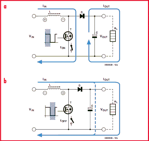
Рис.1. Принцип работы повышающего преобразователя напряжения.
Рис.2 показывает соотношение между выходным напряжением VOUT и временем переключения транзистора (tON и tOFF). С короткими временами tOFF важно использовать диод и конденсаторы с малыми потерями, чтобы гарантировать, что они не превышают их SOA (Безопасная Рабочая Зона), иначе высокая передача энергии может привести к нагреву и выходу из строя.
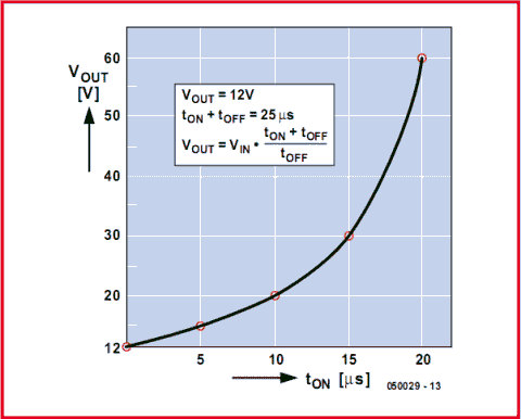
Рис.2
Форма тока и форма волны напряжения показана на рис.3. Форма волны C показывает волновой ток катушки, повышение размера катушки должно уменьшить пульсацию но должно также увеличивать физический размер устройства. Важно гарантировать, что катушка не сделана настолько маленькой, что это не может поставлять достаточную энергию в течение фазы; это произвело бы выходное напряжение с очень слабым регулированием. В нашем устройстве использована катушка 56мкГн.
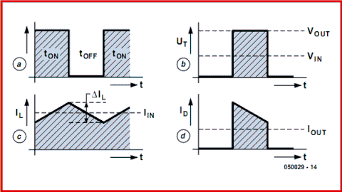
Рис.3
COMPONENTS LIST
Resistors:
R1 = 5kΩ6
R2 = 51kΩ (51kΩ1)
R3 = 9kΩ1 (9kΩ09)
R4 = 1MΩ
R5 = 4kΩ7
R6,R8 = 15kΩ
R7 = 27kΩ
R9,R10 = 6Ω8
R11 = 10kΩ
R12 = 100Ω
P1 = 5kΩ preset
Capacitors:
C1-C4 = 3300µF 16V, radial, low ESR, diam. 12.5 mm, e.g. Panasonic EEUFC1C332 (Farnell)
C5,C10 = 1µF MKT, lead pitch 5mm or 7.5mm (larger version preferred)
C12 = 1µF MKT, lead pitch 5 mm
C6-C9 = 2200µF 25V radial, low ESR, diam. 12.5mm, e.g., EEUFC1E222 (Farnell)
C11 = 22nF, lead pitch 5mm
C13 = 2nF2, lead pitch 5mm
C14,C15 = 100nF ceramic, lead pitch 5mm
C16 = 10µF 63V radial
Inductors:
L1 = 56µH, 21 turns 10 x 0.5 mm ECW, parallel
1 x ETD 29 coil forner, vertical mounting, Epcos B66359X1014T1 (Schuricht # 331622)
2 x ETD 29 clamp, Epcos B66359- A2000 (Schuricht # 333862)
2 x ETD 29 core half, material # N67, air gap 0.5mm, Epcos
B66358-G500-X167 (Schuricht # 333840)
Semiconductors:
D1 = MBR1645 (International Rectifier) (e.g. Reichelt, Segor)
T1 = IRL2505 (International Rectifier) TO-220AB case, (e.g., RS Components)
T2 = BD139
T3 = BD140
IC1 = UC3843N (Texas Instruments) (e.g. Reichelt, Segor)
Miscellaneous:
K1-K4 = 2-way spade terminal, vertical, PCB mount
F1 = fuse, 10A/T (slow) 6.3 x 32 mm (
1⁄4 x 1 1/4 inch) + 2 fuse holdersfor 6.3 mm diameter and PCB mounting
2 x heatsink type SK104-STC (or STS) TO220 38.1mm, 11K/W (Fischer Electronic)Isolating washers for T1
and D1 (TO-220AB) + isolating bushes PCB, order code 050039-1 (see Elektor Shop pages or
)
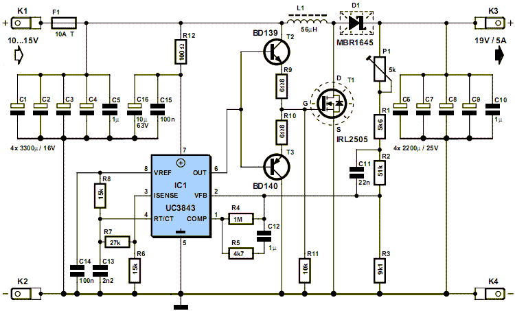
Рис. 4. Принципиальная схема преобразователя напряжения для ноутбука.
Just one IC
The input voltage in the range from 10 to 15 V is connected to terminals K1 and K2 in the circuit diagram (Figure
4). A PCB mounted fuse is fitted in line with the positive supply and the specified fuse holder is equipped with two solder tags for each of the two fuse contact clips, these help to reduce the resistance of the fuse assembly which is particularly important because it passes a high current. Four electrolytic capacitors (C1 to C4) buffer the input voltage. The adapter circuit switches the supply current very quickly and requires special low-loss capacitors suitable for use in switched mode power supplies, the internal impedance of normal electrolytics is too high, they would overheat and may burst. C5 decouples any high frequency signals on the supply voltage.
The coil (L1) is made up from several lengths of enamel covered wire connected in parallel to reduce the skin effect which becomes a problem with high switching speed. The high power switching element is a HEXFET made by International Rectifier. This device has source/drain resistance of just 8 мОм when it is conducting. The low resistance ensures very low power dissipation in the device and allows it to switch a hefty 104 A maximum which should ensure reliable operation in our application. Both the HEXFET and diode are fitted with finned heat sinks. Schottky diode D1 has a TO 220 pack- age outline. It has a 45 V maximum operating voltage and a current of 16 A which gives a forward voltage drop of around 0.63 V, again for reliability the device is conservatively rated. Low ESR type electrolytic capacitors are specified again for output smoothing capacitors C6 to C9. Capacitor C10 is used for high frequency decoupling and the regulated 19 V is output from connectors K3 and K4.
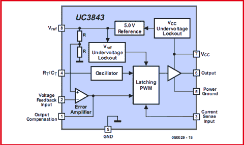
Рис.5
A block diagram of the UC3843 (IC1) is shown in Figure 5. It contains a pulse width modulated (PWM) controller output signal and an internal voltage reference. The adapter output voltage is divided down by R1, R2, R3 and P1 and connected to the voltage feedback input (pin 2) of the controller IC (the error amplifier inverting input). C2 improves the amplifier stability as does R4, R5 and C12 connected between the output (Pin1) and non inverting input of the difference amplifier. The IC clock frequency is defined by the RC network formed by R8 and C13. The component values shown give an oper- ating frequency of around 42 kHz. C14 provides decoupling of the internal ref- erence voltage at pin 8. The supply decoupling network formed by R12, C15 and C16 on the supply pin 7 is important for reliable operation of IC1. The current sense input (pin 3) is not used in this application.
The power FET has a gate capacitance of around 5,000 pF which must be charged and discharged 42,000 times per second if the FET is to be switched successfully. It is important that the transition between on and off occurs as quickly as possible so that there is minimum dissipation in the FET. It is therefore necessary to use a low impedance driver (T2 and T3) between the PWM output of IC1 and the gate pin of the FET. The BD139 and BD140 complimentary pair can handle around 1.5 A limited by resistors R9 and R10. R11 will turn off T1 if for any reason both T2 and T3 become non-conducting or IC1 is defective.
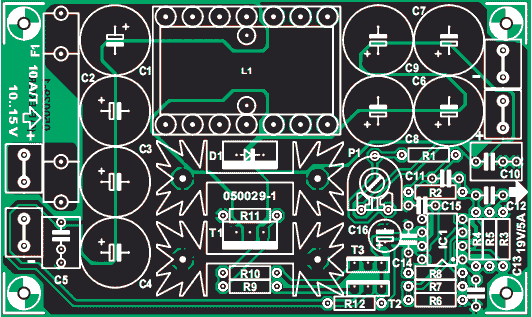
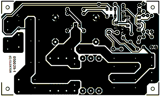
Рис.6
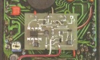
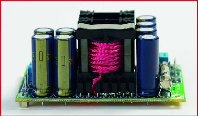
Printed circuit board
The complete circuit fits on the singlsided PCB (Figure 6) without the need for any wire links. Before any of the components are fitted it is best to construct the coil. The PCB layout also includes pads for an off-the-shelf 56 µH inductor but it must be able to handle the high switching currents. The prototype circuit used a coil with an ETD 29 core and was constructed as follows:
The coil has a total of urns but to make things a bit more interesting the wire consists of 10 strands of 0.5 mm diameter enamelled copper wire (ECW) connected in parallel. The effective cross sectional area of all the strands is 1.96 mm2. This method of construction produces a coil with much better properties at this switch- ing speed than would be achieved with a single wire with a cross sec- tional area of 1.96 mm2 (the skin effect has less influence).
The strands are first carefully twisted together before they are soldered to the coil termination posts, if the twist- ing is too tight the there will not be enough space to fit all the 21 turns. Each strand is 2 m long so overall 20 m of 0.5 mm enamel covered wire will be required. The start of the windings are soldered to the first four pins on one side of the coil former and after winding the ends are soldered to the first four pins on the other side of the former. It will be necessary to remove the enamel covering and tin the ends of the wire before they are soldered to the pins. Be careful here because the plastic coil former is not particularly tolerant to high temperatures and the pins may move out of position if the plastic is allowed to get too hot. The seven pins can be supported while soldering by fitting them into a spare strip of perforated prototyping board. For the prototype three layers were necessary for the 21 turns, the first and second layer both comprise of eight turns with five turns left for the last layer. Once the windings are finished and before the end of the windings are soldered in place try assembling the core pieces to make sure there is enough room. When there is insufficient space you can leave off the final turn; 20 turns instead of 21 will not make a lot of difference to the unit’s performance. Alternatively, you can remove one strand from the coil wire so that there are nine rather than ten strands. The coil can also be wound with 16 strands of 0.4 mm ECW (effective cross sectional area of 2.01 mm2) or RF braid provided that the cross sectional area is around 2mm2.
When the winding is complete a layer of insulating tape is wound around the coil. Standard insulating tape is suitable here; the coil temperature never exceeds hand-warm during operation. The parts list specifies two identical core halves with a 0.5 mm gap, once the coil is assembled the total air gap is 1 mm. If you use core halves without any air gap it will be necessary to separate the two halves with some 0.5 mm thick non-conducting material in order to achieve the 1 mm air gap.
Larger outline capacitors were chosen for C5 and C10 with a lead spacing of 7.5 mm, these are better at handling high current and have lower losses.
Begin assembly by fitting the resistors to the PCB then the fuse holder, next comes the spade connectors then the preset followed by the electrolytic capacitors (observe correct polarity) and the coil assembly.
Before the FET and diode are soldered into the PCB a bend should be introduced in the leads to help reduce the mechanical stresses on the soldered joints when the device heats up. Both semiconductors must be insulated fromtheir heat sink using insulating washers and an insulated bush for the M3 mounting bolts and don’t forget to apply a little thermal compound.
Ensure that these devices are well soldered in place because the leads will be carrying several amps. The heatsink can be taller, i.e., 50.8 or 63.5 mm with 9 K/W or 8 K/W respectively. The prototype is fitted with 38.1 mm high heat sink at 11 K/W. From the efficiency viewpoint it would be better if the diode had a smaller heat sink because the diode’s forward conduction voltage decreases with increasing temperature.
However a smaller heat sink may lead to overheating if the output is overloaded. A 20TQ045 diode from IRF can be substituted for D1; this device has a slightly smaller forward voltage drop.
There is no advantage in letting the FET run warmer, its channel resistance (RDSon) increases with increasing temperature. Finally fit transistors T2 and T3 along with IC1 and take the opportunity to double check all the components and soldering before you move on to the next phase and connect power to the adapter.
Power on
Before the unit is powered up for the first time turn the preset P1 fully clockwise to produce the minimum output voltage. For testing use either a power supply capable of supplying 12 V at 10 A or a 12 V vehicle battery. Initially adjust the power supply current limit to 200 mA or, if you are using a battery, connect a 5 W resistor (47 or 56 ?) in series with the positive supply lead to the adapter. Double check that the positive lead of the power supply is connected to K1 and the negative lead to
K2 (nearest to the PCB corner). When no obvious malfunction occurs with the power connected (no excess current drawn from the supply and no smoke signals…) the current limit can be increased (or the series resistor removed). Connect a multimeter to the adapter output connections K3 and K4 (the negative terminal is nearest the board corner again) and check that the output voltage lies in the range of 18 to 19 V. With no load connected to the adapter slowly adjust P1 to ensure that it can achieve an output voltage of 19.4 V. Now use either an electronic load or a combination of high power resistors (4.8 ? at 100 W) and adjust P1 for 19 V output voltage at full load (5 A).
You may notice that when the adapter is operating under full load conditions the by 1 V whenever the load is discon- nected. The output quickly returns to its regulated level and in practice this design ‘feature’ is not a problem for a laptop adapter application.
The finished unit can be mounted in an enclosure. The high efficiency achieved by this design means that very little heat is produced by the unit and there is no need for a fan. A few holes in the case will be sufficient just to allow a little air circulation. Before the unit is connected to the cigarette lighter socket make sure that it (and the plug) are capable of handling 10 A. Connect the adapter to the PC with a suitable lead and connector, double check that the plus and minus are con- nected to the correct input pin of the laptop or notebook PC — never assume that it is equipped with reverse voltage protection!
Michael Schon
schoen.michael@inode.at
| Отправитель | Нити |
|---|


| Ответы | Отправитель | Отправлено |
|---|---|---|
| |
alexfloka | 01.02.2010 11:49 |
| |
vicsen | 09.02.2010 10:34 |
| |
evildesign | 09.02.2010 11:00 |
| |
vicsen | 09.02.2010 11:15 |
| |
evildesign | 09.02.2010 11:36 |
| |
alexfloka | 10.02.2010 10:20 |
| |
evildesign | 10.02.2010 16:53 |
| |
alexfloka | 10.02.2010 17:09 |
| |
evildesign | 10.02.2010 17:34 |
| |
alexfloka | 10.02.2010 18:29 |
| |
evildesign | 10.02.2010 18:39 |
| |
vicsen | 10.02.2010 22:02 |
| |
alexfloka | 11.02.2010 18:05 |
| |
Wind | 02.03.2010 14:47 |
| |
MACTEP | 02.03.2010 18:14 |
| |
Mihail123 | 31.08.2010 21:30 |
| |
MACTEP | 01.09.2010 17:02 |
| |
Mihail123 | 01.09.2010 21:25 |
| |
MACTEP | 01.09.2010 21:38 |
| |
Mihail123 | 01.09.2010 21:43 |
| |
MACTEP | 01.09.2010 21:44 |
| |
Mihail123 | 01.09.2010 21:51 |
| |
MACTEP | 01.09.2010 21:57 |